| APPLICATION NOTE USM 105 | Author: Mihaela Radulescu, M Physic. Sc. member technical staff, SEMICONIX CORPORATION |
| The Spiral Inductors are essential for bias injection into oscillators, amplifiers and microwave switches. They can also be used to bias tuning varactors, PIN diodes, transistors and monolithic circuits. The parameters of interest for the design of inductors are its inductance (L), quality factor (Q) and self resonant frequency (SRF). Unfortunately there are no simple formulas to determine them accurately and we enter the realm of simulations and modeling to determine these parameters. There are already many products in the market which model and simulate spiral inductors and planar transformers. Some of them rely on electromagnetic simulation while others use simple lumped element models. The programs which use electromagnetic simulation are very expensive and often take a few hours to days to run a complete simulation. On the other hand, existing lumped element approaches run a first order analysis and do not give an accurate value for the critical parameters like Q and SRF. The options for a designer who wants a quick solution are very limited and one has to make a choice between an expensive electromagnetic simulator and a simulator that doesn't give good results. The design of inductors can be optimized using a combination of full-wave electromagnetic solvers such as method-of-moment based tools (sonnet) and quasi-TEM approaches. SONNET is a suite of products which provides high-frequency planar electromagnetic analysis for different products suitable for passives that use a circular topology. It uses a modified method of moments analysis based on Maxwell's equations to perform a true three dimensional current analysis of predominantly planar structures. Em, the electromagnetic engine, computes S, Y, or Z-parameters, transmission line parameters (Z0 and eeff), and SPICE equivalent lumped element networks. The suite includes a number of tools like emvu and patvu which are visualization tools to help the user better interpret the results. The small disadvantage with this program seems to be the long simulation time depending on the resolution of the mesh used for analysis. Model Overview A scalable physical model that can accurately predict the behavior of inductors with different structural parameters over a broad range of frequency would be a valuable design tool. Each element of the model should be consistent with the physical phenomena occurring in the part of the structure it represents.
Lumped device parameters like the inductance of spiral, the net series resistance of spiral (combining all metal layers of the spiral), the overlap capacitance between the turns of spiral and the cross-under layer, the capacitance between bottom-most layer of the spiral and substrate, the parameter modeling substrate losses and substrate capacitive effects can be expressed vs the physical dimensions of the inductor: N = number of turns, W = width of
metal strip, s = the turn spacing, L = length of spiral, Dout = outer diameter of spiral, Din = inner diameter of spiral, so for a given shape, an inductor is completely specified by its physical dimensions.
A simple approximate expression for the inductance does predict the correct order of magnitude of the inductance with typical errors of 20% or more. In [7] it is described new approximate expressions for the inductance of planar inductors. The first approximation is based on a modification of an expression developed by Wheeler [6]; the second is derived from electromagnetic principles by approximating the sides of the spirals as current-sheets; and
the third is a monomial expression derived from fitting to a large database of inductors (and the exact inductance values). All three expressions are accurate, with typical errors of 2-3%, and very simple, and are therefore excellent candidates for use in design and synthesis.
Where r is the fill ratio defined as (Dout-Din)/(Dout+Din), davg is the average diameter 0.5(Dout+Din) and the coefficients K1 and K2 are layout dependent. |
Two inductors with the same average diameter but different fill ratios will, of course, have different inductance values. The full one has a smaller inductance because its inner turns are closer to the center of the spiral and so contribute
less positive mutual inductance and more negative mutual inductance. Another simple and accurate expression for the inductance of a planar spiral can be obtained by approximating the sides of the spirals by symmetrical current sheets of equivalent current densities The self and mutual inductances are evaluated using the concepts of geometric mean distance (GMD), arithmetic mean distance (AMD), and arithmetic mean square distance (AMSD) [5] The resulting expression is
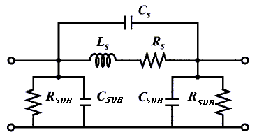
Where the coefficients ci are layout dependent [5]. Although the accuracy of this expression worsens as the ratio s/W becomes large, it exhibits a maximum error of 8% for 3W>=s. Typical practical spiral inductors are built with W>=s. The reason is that a smaller spacing improves the interwinding magnetic coupling and reduces the area consumed by the spiral. A large spacing is only desired to reduce the interwinding capacitance. In practice, this is not a concern as this capacitance is dwarfed by the underpass capacitance. The electrical coupling limits the maximum frequency of operation for the inductor, given by its self-resonance (SRF). In Fig. 1, this effect described by the capacitors. These include the turn-to-substrate capacitance, a capacitance associated with each turn of the metal layer to the substrate and a side-wall capacitance associated between adjacent turns. The series capacitance Cs models the parasitic capacitive coupling between input and output ports of the inductor. This capacitance allows the signal to flow directly from the input to output port without passing through the spiral inductor. Based on the inductor's physical structure, both the crosstalk between adjacent turns and the overlap between the spiral and underpass contribute to Cs. However, since the adjacent turns are almost equipotential, the effect of the crosstalk capacitance is negligible. Furthermore, the crosstalk capacitance can be reduced by increasing the spacing between the turns. The effect of overlap capacitance is more significant because of the larger potential difference between the spiral and the underpass. The series resistance, Rs, takes into account the skin depth of a conductor with finite thickness [3] and the current distribution in a microstrip conductor [4] The series resistance, Rs, can be expressed as
where rm and L represent the resistivity and length of the wire. If t is the physical thickness of the wire, an effective thickness teff can be defined as
d is the skin depth which is the most critical parameter pertaining to eddy current effects and is defined as:
where rm,m and f represent the resistivity in W-m, permeability in H/m, and frequency in Hz, respectively. The skin depth is also known as the "depth of penetration" since it describes the degree of penetration by the electric current and magnetic flux into the surface of a conductor at high frequencies. The severity of the eddy current effect is determined by the ratio of skin depth to the conductor thickness. The eddy current effect is negligible only if the depth of penetration is much greater than the conductor thickness. As d decreases with frequency, increases. The scattering parameters of the spiral inductor may be derived easily from its lumped model which can be visualized as a P-network. Based on this figure, the reactances Y1 , Y2 and Y3 of the spiral can be computed. The Y-parameters of the network are given as follows: Y11=Y2+Y3=Y22 It is now a fairly simple matter to convert these Y-parameters to S-parameters. The conversion relationships are as follows:
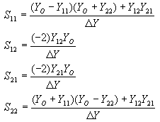
It is now a fairly simple matter to convert these Y-parameters to S-parameters. The conversion relationships are as follows:
Here, DY = (Y11 +Y0)(Y22 +Y0) - Y12Y21 and Y0 is the characteristic admittance of the line. References [1] H. M. Greenhouse, "Design of Planar Rectangular Microelectronic Inductors," IEEE Trans. Parts, Hybrids, and Packaging, v. PHP-10, no.2, June 1974, pp. 101-109 |
 (1)
(1) (6)
(6)