The latest version of a filter
synthesis program for the personal computer supports the creation of microstrip,
stripline, lumped-element, and waveguide filters.
Filter designers have a wide choice of commercial software design tools at their
disposal.But the latest version (Version 3.0) of the MMICAD filter synthesis
software suite from Optotek Ltd. (Kanata, Ontario, Canada) now includes userdefined
physical surroundings as an integral part of the synthesis operation. The software
synthesis tool is actually a set of 35 dedicated programs for the design of
microstrip, lumped element, stripline, and waveguide filters. The design interface
and common menu format seamlessly integrates with the MMICAD linear simulator
and physical layout in a user-friendly design environment. A design example
of a parallel coupled bandpass filter will be illustrated in this article.
The parallel coupled-line bandpass filter is one of the more popular microwave-filter
designs. It is suitable for implementation in microstrip and surface-mount
construction. However, there are practical limitations to its design. Design
bandwidths are limited to about 20 or 30 percent around the center frequency
due to decreasing input
coupling gap that is a function of increasing bandwidth and decreasing passband
ripple. There are also practical considerations in construction that includes
the width of the housing, which should be kept less than onehalf wavelength
of the highest frequency in order to suppress the possibility of the TE01 waveguide
mode propagation
that can propagate energy around the filter 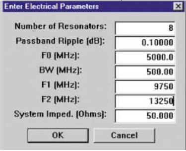
1. This dialog box is used for entering the electrical parameters for the example filter design. and limit the attainable stopband attenuation. The presence of a cover over the circuit can cause the passband frequency to be shifted, and this should be compensated for in the design synthesis. At higher frequencies, microstrip dispersion must be accounted for if the passband is to be centered on the design frequency. Other circuit discontinuities, such as microstrip metalizaztion, and the capacitance at the ends of the coupled resonator lines, must also be included in the filter synthesis.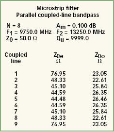
2. This data window shows the calculated even- and odd-mode resonator impedances for the example filter. All of these factors should be included in the synthesis if multiple fabrication trials are to be minimized and possibly eliminated. The interface to the synthesis software, the menu system, is organized and arranged to match the sequence of calculations a designer would normally follow. This gives the designer access to the intermediate steps in the calculations, and allows the designer the opportunity to control, interact, and optimize a design during the calculation process. For example, an electrical design may have been arrived at, and the microstrip dimensions can then be separately calculated and optimized by the designer varying the substrate dielectric constant and thickness, the metal thickness, the cover height, and the type of input coupling. The requirement is for a filter that operates from 10.0 to 13.0 GHz with greater than 30-dB rejection at 9.0 and 14.0 GHz will be used as a design example. 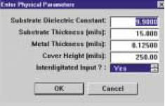
3. Microstrip physical parameters for the filter example are entered into this dialog box. 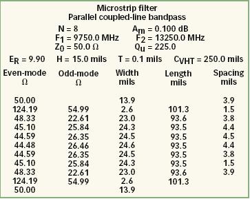
4. This data window shows the calculated microstrip dimensions for the example filter design. A filter with eight resonators and a passband ripple of 0.1 dB (return loss of 16.3 dB) will meet this requirement. The design bandwidth is set to 3.5 GHz centered at 11.5 GHz, which is an F1 of 9.75 GHz and F2 of 13.25 GHz, representing a fractional bandwidth of 30 percent. Figure 1 shows the dialog window for entering electrical information for a desired filter, including the number of resonators, passband ripple, center frequency, bandwidth, rejection frequencies, and impedance. Figure 2 shows the resulting calculated even- and odd-mode impedances for this parallel-coupled-line filter design. The synthesis software can also calculate the filter frequency response, including dissipative losses. The response calculation can be used to verify that the basic electrical design will meet a set of requirements, including the increased passband insertion loss at the band edges due to dissipative losses.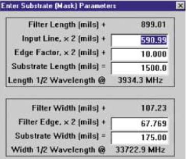
5. This dialog box shows the layout dimensions for the example filter design, along with the calculated waveguide cutoff frequency. |
The calculated response for this design will be generated by Version
3.0 of the MMICAD linear circuit analysis program.5 Figure 3 shows the dialog box for entering the physical parameters
of substrate dielectric constant and thickness, metal thickness, and the type
of input coupling. For this particular filter design, the substrate is 0.015-in.-thick alumina with 0.125-mil-thick thin-film metalization. The unloaded quality factor (Q) for this substrate obtained though experimentis about 225 at X-band. Because of the tight input coupling required for this large bandwidth, interdigitated coupling lines were chosen for this filter. The filter’s calculated dimensions are shown in Fig. 4. For noninterdigitated lines, the line width would be 11.1 mils although the line spacing would be only 0.4 mils, somewhat less practical to fabricate compared to the interdigitated design. In Fig. 5, a dialog box is used for specifying the circuit layout and the circuit mask. There is an intermediate window (not shown) that allows choosing the arrangement of the circuit input and output lines. Here, input and output lines are selected on a common centerline.This produces the narrowest layout and substrate width, and maximizes the TE01 mode cutoff frequency for a metal enclosure. The calculated cutoff frequency is part of the dialog box and is 33.723 GHz for a substrate width of 175 mils. This width is chosen for mechanical packaging purposes. The overall length of the substrate is 1500 mils. Once all required values have been entered into the dialog box, the software yields a circuit layout that can be written to a DXF file for direct generation of the photo mask. A photograph of the filter fabricated from this synthesized file is shown in Fig. 6. The filter-synthesis program generates a series of netlist files with the calculated nominal dimensions of the circuit for design verification, as well as files for analysis of changes in filter response with temperature, files for worst-case and yield analysis, and netlist files of circuit discontinuities to improve performance predictions. 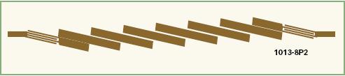
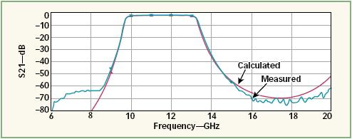
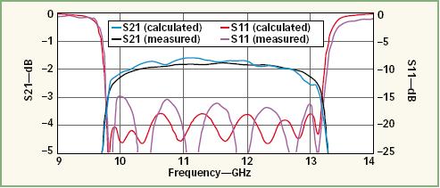
6. This layout artwork offers a representation of the fabricated microstrip filter. Figure 7 gives the filter frequency response calculated by MMICAD over a wide frequency range. The calculation covers the frequency range of 6.0 to 20.0 GHz, and it shows the expected rejection of the filter. Figure 8 gives the calculated response over a narrow band of 9.0 to 14.0 GHz, and this shows the expected passband insertion loss and return loss frequency response.
Fabricated Filter
7. The example filter’s measured response compares closely with the response predicted by the MMICAD software. First, the pairs of interdigitated fingers can resonate in a quarter-wave-length transverse-electromagnetic (TEM) mode and this condition causes a resonancesuck-out in the passband. This was eliminated with bond wires that shorted the tips of the open circuit ends of the fingers. Second, the test fixture itself has a known insertion loss of 0.8 dB, due to SMA connector loss and transition to microstrip loss. Consequently, a 0.8-dB attenuator is added to the filter circuit netlist to make the calculated losses match the measured. It is apparent that the measured rounding of the passband, the result of filter resonator dissipative losses, matches the calculated. The passband return loss is better than –15 dB, compared to the design value of –16.3 dB. And third, the measured results are for the first fabrication of this filter without any tuning or modifications. The measured data for the fabricated filter is in excellent agreement with both the design goals and with the MMICAD simulation of the circuit synthesized dimensions. Only part of the reason for this success is the relatively tight tolerances that are possible with thin-film alumina microstrip.
8. The measured insertion loss and return loss for the example filter compares closely with the responses calculated by the MMICAD software. The excellent circuit performance is possible because the synthesis includes compensation of those circuit details that can alter and degrade the response. Furthermore, the MMICAD synthesis software facilitates design trade-offs as part of the synthesis process and it facilitates detailed circuit analysis by creating the necessary MMICAD netlists. ACKNOWLEDGMENT |