|
LOW OFFSET VOLTAGE DUAL COMPARATOR
USM LM 393
FEATURES
APPLICATIONS
VOLTAGE REGULATOR
Wide single supply 2.0V to 36V
Dual supplies:±1.0V to ±18V
Very low supply current drain (0.4 mA) independent of supply voltage
In DIE form, this device is an excellent selection for many chip and wire HYBRID CIRCUITS
PRODUCT DESCRIPTION AND SHORT APPLICATION NOTE
The USM LM393 series are dual independent precision voltage comparators capable of single or split power supply operation. These devices are designed to permit a common mode range to ground level with single supply operation.
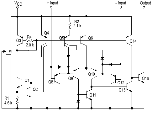
IC SCHEMATIC DIAGRAM
MAXIMUM RATINGS
PARAMETER SYMBOL VALUE UNITS
Power Supply Voltages VCC +36 or ±18 Vdc
Input Differential Voltage Range VDIR 32 Vdc
Input Common Mode Voltage Range VICR -0.3 to +36 Vdc
Output Short Circuit–to–Ground
Output Sink Current (Note 1) ISC
ISINK Continuous
20 mA
Power Dissipation TA=25 °C
Derate above 25°C PD
1/RthJA 570
5.7 mW
mW/°C
Operating Ambient Temperature Range TA -25 to +85 °C
Maximum Operating Junction Temperature TJ(MAX) 125 °C
Storage Temperature Range TSTG -65 to 150 °C
ONLY Proper die handling equipment and procedures should be employed. Stresses beyond listed absolute maximum ratings may cause permanent damage to the device.
ELECTRICAL CHARACTERISTIC
VCC=5.0Vdc, Tlow=15kW, VCC=15Vdc, TA=25°C 50 200 V/mV
Large Signal Response Time Vin=TTL Logic Swing, Vref=1.4 Vdc
VRL=5.0 Vdc, RL=5.1kW, TA=25°C 300 ns
Response Time(Note5) VRL=5.0 Vdc, RL=5.1kW, TA=25°C 1.3 µs
Input Differential Voltage (Note 6) Vin>= GND or V– Supply (if used) VCC V
Output Sink Current Vin>=1.0Vdc, Vin+=0Vdc, VO<1.5Vdc 6.0 16 mA
Output Saturation Voltage TLow=1.0 Vdc, Vin+=0 Vdc, ISink<4.0mA 150
- 400
700
*Tlow=0°C, Thigh=+70°C
(NOTE 1)The maximum output current may be as high as 20 mA, independent of the magnitude of VCC, output short circuits to VCC can cause excessive heating and eventual destruction.
(NOTE 2)At output switch point, VO= 1.4 Vdc, RS=0 with VCC from 5.0 Vdc to 30 Vdc, and over the full input common mode range (0 V to V=–1.5 V).
(NOTE 3)Due to the PNP transistor inputs, bias current will flow out of the inputs. This current is essentially constant, independent of the output state, there fore, no loading changes will exist on the input lines.
(NOTE 4)Input common mode of either input should not be permitted to go more than 0.3 V negative of ground or minus supply. The upper limit of common mode range is V CC–1.5 V.
(NOTE 5)5.Response time is specified with a 100 mV step and 5.0 mV of overdrive. With larger magnitudes of overdrive faster response times are obtainable.
(NOTE 6)The comparator will exhibit proper output state if one of the inputs becomes greater than Vrange. The low input state must not be less than –0.3 V of ground or minus supply.
GENERAL DIE INFORMATION
Substrate Thickness (mils) Die size (mils) [mm] Bonding pads(mils) Backside metal
Silicon 10±1 (51.181x47.244) [1.3x1.2] 4.724x4.724 Backside of the die is coated with 0.5µm GOLD , which makes it compatible with AuSi or AuGe die attach.
All US Microwaves products are available in die form. Typical delivery for die products is 2-3 weeks ARO. For Custom designs, delivery is 3-4 weeks ARO. Certain items may be available from stock. Inventory is periodically updated. All devices for chip and wire applications are 100% tested, visual inspected and shipped in waffle packs (WP). For high volume automated assembly, MIS chip capacitors are supplied as 4" wafers 100% tested, inked and diced on expanded film frame (FF).
TECHNOLOGY DESCRIPTION: SEMICONDUCTOR-MANUFACTURING
These integrated Circuits are manufactured with medium voltage junction isolated bipolar process. junction isolated bipolar processes allow integration of high performance NPN, PNP and JFET transistors, MOS capacitors, diffused resistors and precision thin film resistors. The bond pad metallization is standard 1µm Aluminium. The backside of the die is coated with 0.5µm GOLD , which makes it compatible with AuSi or AuGe die attach.
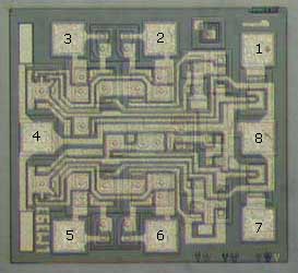
DIE LAYOUT - MECHANICAL SPECIFICATIONS
PAD # FUNCTION X(mils) X(mm) Y(mils) Y(mm)
1 #1 OUT 42.322 1.075 36.322 0.920
2 #1 IN- 25.393 0.645 37.972 0.965
3 #1 IN+ 9.448 0.240 37.972 0.965
4 GND 3.937 0.100 21.062 0.535
5 #2 IN+ 9.448 0.240 3.937 0.100
6 #2 IN- 25.393 0.645 3.937 0.100
7 #2 OUT 42.322 1.075 5.905 0.150
8 VCC 42.322 1.075 20.866 0.530
STANDARD PRODUCTS ORDERING INFORMATION
STANDARD PRODUCTS PRICE LIST
USM PART # MINIMUM ORDER QUANTITY Waffle Packs U/P($)
USMLM393 100pc -WP $3.20
List prices are for standard products, available from stock.
List prices for other quantities and tolerances are available on line through Instant Quote.
For standard products available from stock, there is a minimum line item order. For custom products
please inquire by contacting US Microwaves technical sales. No rights can be derived from pricing
information provided on this website. Such information is indicative only, is showed for budgetary
use only and subject to change by US MICROWAVES at any time and without notice.
Products sold for space, military or medical applications, element evaluation and/or level K or S qualification are subject to minimum order levels to be established on a case by case basis. For any special applications, die level KGD qualification requirements, different packaging or custom configurations, contact sales department.
INSTANT QUOTE
US Microwaves P/N Quantity E-mail
ORDERING: Order on line at: http://www.usmicrowaves.com/porder.htm. A copy of the order along with an order confirmation receipt is issued instantly for all orders placed on line. On line Orders have to be verified, accepted and acknowledged by US Microwaves sales department in writing before, becoming non cancelable binding contracts.
DELIVERY: Typical delivery for die products packaged in waffle packs is 2-4 weeks ARO. For Custom designs, delivery is 3-5 weeks ARO. Certain items may be available from stock with delivery up to 1 week.
SHIPPING/PACKAGING: All devices for chip and wire applications are 100% tested, visual inspected and shipped in waffle packs (WP).
SAMPLES: Samples are available only for customers that have issued firm orders pending qualification of product in a particular application.
GUARANTEED SUPPLY! US Microwaves guarantees continuous supply and availability of all standard products provided minimum order quantities are met.
U.S. Microwaves has made every effort to have this information as accurate as possible. However, no responsibility is assumed by U.S. Microwaves for its use, nor for any infringements of rights of third parties which may result from its use. U.S. Microwaves reserves the right to revise the content or modify its product line without prior notice. U.S. Microwaves products are not authorized for and should not be used within support systems which are intended for surgical implants into the body, to support or sustain life, in aircraft, space equipment, submarine, or nuclear facility applications without the specific written consent of U.S. Microwaves.
|