|
HIGH PERFORMANCE CURRENT MODE CONTROLLERS
USM UC3842A
FEATURES
APPLICATIONS
HIGH PERFORMANCE CURRENT MODE CONTROLLERS
Trimmed Oscillator Discharge Current for Precise Duty Cycle Control
Current Mode Operation to 500 kHzAutomatic Feed Forward Compensation
Latching PW°M for Cycle–By–Cycle Current Limiting
Internally Trimmed Reference with Undervoltage Lockout
High Current Totem Pole Output Undervoltage Lockout with Hysteresis
Low Startup and Operating CurrentDirect Interface with Motorola SENSEFET Products
In DIE form, this device is an excellent selection for many chip and wire HYBRID CIRCUITS
PRODUCT DESCRIPTION AND SHORT APPLICATION NOTE
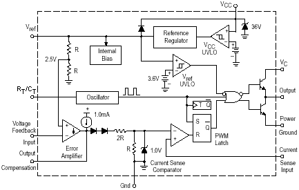
The USM UC3842A series of high performance fixed frequency current mode controllers are specifically designed for off–line and dc–to–dc converter applications offering the designer a cost effective solution with minimal external components. These integrated circuits feature a trimmed oscillator for precise duty cycle control, a temperature compensated reference, high gain error amplifier, current sensing comparator, and a high current totem pole output ideally suited for driving a power MOSFET.Also included are protective features consisting of input and reference under-voltage lockouts each with hysteresis, cycle–by–cycle current limiting, programmable output deadtime, and a latch for single pulse metering. These devices are available in die form. The UC3842A has UVLO thresholds of 16 V (on) and 10 V (off), ideally suited for off–line converters.
IC SCHEMATIC DIAGRAM
MAXIMUM RATINGS
PARAMETER SYMBOL VALUE UNITS
Total Power Supply and Zener Current ICC+IZ 30 mA
Output Current, Source or Sink (Note 1) IO 1.0 A
Output Energy (Capacitive Load per Cycle) W 5.0 µJ
Current Sense and Voltage Feedback Inputs Vin -0.3 to+5.5 V
Error Amp Output Sink Current IO 10 mA
Power Dissipation PD 1 W
Operating Junction Temperature TJ 150 °C
Operating Ambient Temperature TA 0 to +70 °C
Storage Temperature Range Tstg -65 to 150 °C
ONLY Proper die handling equipment and procedures should be employed. Stresses beyond listed absolute maximum ratings may cause permanent damage to the device.
ELECTRICAL CHARACTERISTIC
VCC=15V[note2], RT=10k, CT=3.3nF, TA=Tlow to Thigh [Note3]
PARAMETER TEST CONDITIONS SYMBOL MIN TYP MAX UNITS
Reference Output Voltage Io=1mA,TJ=25°C VREF 4.95 5.00 5.05 V
Line Regulation VCC=12V to25V Regline - 2.0 20 mV
Load Regulation IO=1.mA to 20mA Regload - 3.0 25 mV
Temperature Stability TS 0.2 mV/°C
Total Output Variation over Line, Load, Temperature Vref 4.9 5.1 V
Output Noise Voltage (f=10 Hz to 10 kHz, TJ=25°C) Vn 50 µV
Long Term Stability (TA=125°C for 1000 Hours) S 5.0 mV
Output Short Circuit Current ISC -30 -85 -180 mA
Frequency TJ=25 °C
TA=Tlow to Thigh fOSC 47
46 52
- 57
60 kHz
Frequency Change with Voltage VCC=12V to 25V DfOSC/DV 0.2 1.0 %
Frequency Change with Temperature TA=Tlow to Thigh DfOSC/DT 5.0 %
Oscillator Voltage Swing (Peak-to-Peak) VOSC 1.6 V
Discharge Current VOSC=2.0V
TJ=25°C
TA=Tlow to Thigh Idischg 7.5
7.2 8.4
- 9.3
9.5 mA
Voltage Feedback Input VO=2.5V VFB 2.45 2.5 2.55 V
Input Bias Current VFB=2.7V IIB -0.1 -1.0 mA
Open Loop Voltage Gain VO=2.0V to 4.0V AVOL 65 90 dB
Unity Gain Bandwidth TJ=25 °C BW 0.7 1 MHz
Power Supply Rejection Ratio VCC=12V to 25V PSSR 60 70 dB
Output Current sink(VO=1.1V VFB=2.7V)
source(VO=5.0V VFB=2.3V) ISink
ISource 2.0
-0.5 12
-1.0 mA
Output Voltage Swing High state(RL=15ktoground,VFB=2.3V)
Low state(RL=15k toVref,VFB=2.7V )
VOH
VOL 5.0
- 6.2
0.8 -
1.1 V
Current Sense Input Voltage Gain (Notes 4 & 5) AV 2.85 3.00 3.15 V/V
Maximum Current Sense Input Threshold (Note 4) Vth 0.9 1.0 1.1 V
Power Supply Rejection Ratio VCC=12V to 25V PSSR 70 dB
Input Bias Current IIB -2.0 -10.0 mA
Propagation Delay (Current Sense Input to Output) tPLH(IN/OUT) 150 300 ns
Output Voltage Low state(ISink=200mA)
(ISink=200mA)
High state(ISink=20mA)
(ISink=200mA) VOL
VOH -
-
13
12 0.1
1.6
13.5
13.4 0.4
0.2
-
- V
Output Voltage with UVLO Activated VCC=6.0 V ISink=1.0 mA VOL(UVLO) 0.1 1.1 V
Output Voltage Rise Time CL=1nF TJ=25 °C tr 50 150 ns
Output Voltage Fall Time CL=1nF TJ=25 °C tf 50 150 ns
Startup Tresholde Vth 15 16 17 V
Minimum OperatingVoltage After Turn-on VCC(min) 9 10 11 V
Duty Cycle
Maximum
Minimum
DCmax
DCmin 94
- 96
- -
0 %
Power Supply Current(Note 2) VCC=14V ICC 12 17 mA
Power Supply Zenner Voltage ICC=25mA VCC 30 36 V
(NOTE 1)Maximum Package power dissipation limits must be observed.
(NOTE 2)Adjust Vcc above the Startup threshold before setting to 15 V.
(NOTE 3)Low duty cycle pulse techniques are used during test to maintain junction temperature as close to ambient as possible Tlow=0°C Thigh=+70°C.
(NOTE 4)This parameter is measured at the latch trip point with VFB=0°V
(NOTE 5)Comparator gain is defined as: AV*(DV Output Compensation)/(DVCurrent Sense Input)
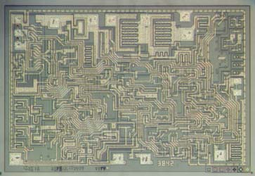
GENERAL DIE INFORMATION
Substrate Thickness (mils) Die size (mils) [mm] Bonding pads Backside metal
Silicon 10±1 (93.7x64.8) [2.38x1.63] min 4x4 mils, 1µm thick, aluminium Backside of the die is coated with 0.5µm GOLD , which makes it compatible with AuSi or AuGe die attach.
All US Microwaves products are available in die form. Typical delivery for die products is 2-3 weeks ARO. For Custom designs, delivery is 3-4 weeks ARO. Certain items may be available from stock. Inventory is periodically updated. All devices for chip and wire applications are 100% tested, visual inspected and shipped in waffle packs (WP). For high volume automated assembly, MIS chip capacitors are supplied as 4" wafers 100% tested, inked and diced on expanded film frame (FF).
TECHNOLOGY DESCRIPTION: SEMICONDUCTOR-MANUFACTURING
These integrated Circuits are manufactured with medium voltage junction isolated bipolar process. junction isolated bipolar processes allow integration of high performance NPN, PNP and JFET transistors, MOS capacitors, diffused resistors and precision thin film resistors. The bond pad metallization is standard 1µm Aluminium. The backside of the die is coated with 0.5µm GOLD , which makes it compatible with AuSi or AuGe die attach.
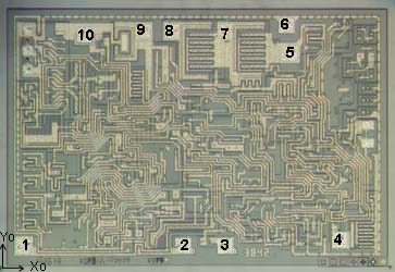
DIE LAYOUT - MECHANICAL SPECIFICATIONS
PAD # FUNCTION X(mils) X(mm) Y(mils) Y(mm)
1 Comp 0.09 3.543 0.11 4.330
2 VFB 1.05 41.338 0.11 4.330
3 Isense 1.31 51.575 0.11 4.330
4 RT/CT 2.00 78.740 0.15 5.905
5 Power GND 1.70 66.929 1.28 50.394
6 GND 1.68 66.142 1.45 57.087
7 OUT 1.31 51.575 1.41 55.512
8 Power Vcc 0.99 38.976 1.41 55.512
9 Vcc 0.815 32.087 1.41 55.512
10 Vref 0.46 18.110 1.39 54.724
STANDARD PRODUCTS ORDERING INFORMATION
STANDARD PRODUCTS PRICE LIST
USM PART # MINIMUM ORDER QUANTITY Waffle Packs U/P($)
USMUC3842A 100pc -WP $3.20
List prices are for standard products, available from stock.
List prices for other quantities and tolerances are available on line through Instant Quote.
For standard products available from stock, there is a minimum line item order. For custom products
please inquire by contacting US Microwaves technical sales. No rights can be derived from pricing
information provided on this website. Such information is indicative only, is showed for budgetary
use only and subject to change by US MICROWAVES at any time and without notice.
Products sold for space, military or medical applications, element evaluation and/or level K or S qualification are subject to minimum order levels to be established on a case by case basis. For any special applications, die level KGD qualification requirements, different packaging or custom configurations, contact sales department.
INSTANT QUOTE
US Microwaves P/N Quantity E-mail
ORDERING: Order on line at: http://www.usmicrowaves.com/porder.htm. A copy of the order along with an order confirmation receipt is issued instantly for all orders placed on line. On line Orders have to be verified, accepted and acknowledged by US Microwaves sales department in writing before, becoming non cancelable binding contracts.
DELIVERY: Typical delivery for die products packaged in waffle packs is 2-4 weeks ARO. For Custom designs, delivery is 3-5 weeks ARO. Certain items may be available from stock with delivery up to 1 week.
SHIPPING/PACKAGING: All devices for chip and wire applications are 100% tested, visual inspected and shipped in waffle packs (WP).
SAMPLES: Samples are available only for customers that have issued firm orders pending qualification of product in a particular application.
GUARANTEED SUPPLY! US Microwaves guarantees continuous supply and availability of all standard products provided minimum order quantities are met.
U.S. Microwaves has made every effort to have this information as accurate as possible. However, no responsibility is assumed by U.S. Microwaves for its use, nor for any infringements of rights of third parties which may result from its use. U.S. Microwaves reserves the right to revise the content or modify its product line without prior notice. U.S. Microwaves products are not authorized for and should not be used within support systems which are intended for surgical implants into the body, to support or sustain life, in aircraft, space equipment, submarine, or nuclear facility applications without the specific written consent of U.S. Microwaves.
|