| ELECTRICAL CHARACTERISTIC |
| VI=14.4V;CO=100F;Tj=25°C unless otherwise specified. |
| PARAMETER |
TEST CONDITIONS |
MIN |
TYP |
MAX |
UNITS |
| Output Voltage |
-25°C =<TJ =<85°C
Full Operating temperature
1mA =< IL =< 400mA, TJ =< TJMAX |
0.985|VO|
0.98|VO|
0.975|VO| |
VO
VO |
1.015|VO|
1.02|VO|
1.025|VO| |
V |
| Input Supply Voltage |
|
|
|
26 |
|
| Output Voltage Temperature Coefficient |
(Note 1) |
|
50 |
150 |
ppm/°C |
| Line Regulation (Note 2) |
13V =< Vin =< 26V (Note 3) |
|
0.1 |
0.4 |
% |
| Load Regulation (Note 2) |
1mA=<IL =< 400mA |
|
0.1 |
0.3 |
% |
| Dropout Voltage (Note 4) |
IL = 150mA
IL = 400mA |
|
200
420 |
400
700 |
mV |
| Ground Current (Note 5) |
IL = 100mA
IL = 150mA
IL = 400mA |
|
100
12
30 |
200
20
50 |
µA
mA
|
| Dropout Ground Current (Note 5) |
Vin = Vout - 0.5V,
IL = 150mA |
|
110 |
120 |
µA |
| Current Limit |
Vout = 0 |
|
350 |
500 |
mA |
| Thermal Regulation (Note 6) |
|
|
0.05 |
0.2 |
%/W |
| Output Noise, 10Hz to 100KHz IL = 100mA |
CL = 2.2µF
CL = 3.3µF
CL = 33µF |
|
500
350
120 |
|
µVRMS
|
| Ripple Rejection Ratio |
IO = 350mA, f = 120Hz, CO = 100µF,
Vin = VO + 3V + 2Vpp |
60
|
|
|
dB |
|
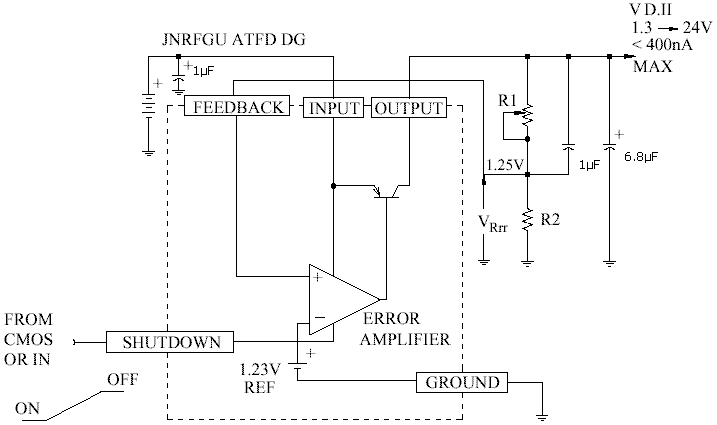
Adjust model
|
|
Reference Voltage
|
Over Temperature (Note 7)
|
1.21
1.185 |
1.235 |
1.26
1.285 |
V
|
|
Feedback Pin Bias Current
|
|
|
20 |
40 |
nA |
|
Reference Voltage Temperature Coefficient
|
(Note 1)
|
|
50 |
|
ppm/°C |
|
Feedback Pin Bias Current Temperature Coefficient
|
|
|
0.1 |
|
nA/°C |
|
Shutdown Input
|
|
Input Logic Voltage
|
Low (Regulator ON)
High (Regulator OFF)
|
2 |
1.3
|
0.7
|
V
|
|
Shutdown Pin Input Current
|
Vs = 2.4V
Vs = 26V
|
|
30
450 |
50
600 |
µA
|
|
Regulator Output Current in Shutdown
|
(Note 8)
5.0V =< Vout < 15.0V
3.3V =< Vout < 5.0V
2.0V =< Vout < 3.3V
|
|
|
10
20
30 |
|
| |
| (NOTE 1) Output or reference voltage temperature coefficients defined as the worst case voltage change divided by the total temperature range. |
| (NOTE 2) Regulations is measured at constant junction temperature, using pulse testing with a low duty cycle. Changes in output voltage due to heating effects are covered under the specification for the thermal regulation. |
| (NOTE 3) Line regulation is tested at 150°C for IL = 5mA. For IL = 100mA and TJ = 125°C. line regulation is guaranteed by design to 0.2%. For USM4815 16 =< VIN =< 26V. |
| (NOTE 4) Dropout voltage is defined as the input to output differential at which the output voltage drops 2% below its nominal value measured at 1V differential. |
| (NOTE 5) Ground pin current is the regulator quiescent. The total current drawn from the sources is the sum of the ground pin current and output load current. |
| (NOTE 6) Thermal regulation is the change in output voltage at a time T after a change in power dissipation, excluding load or line regulation effects. Specifications are for a 200mA load pulse (3W pulse) for T = 10ms. |
| (NOTE 7) Vref =< Vout =< (Vin - 1V), 2.3V =< Vin =< 26V, 100m =< IL =< 400mA, TJ =< TJMAX. |
| (NOTE 8) Vshutdown >= 2V, Vin >= 26V, Vout = 0V. |
| STANDARD PRODUCTS PRICE LIST |
| USM PART # |
MINIMUM ORDER QUANTITY |
Waffle Packs |
U/P($) |
| USM L48XX-ADJ |
100pc |
-WP |
$3.20 |
| List prices are for standard products, available from stock.
List prices for other quantities and tolerances are available on line through Instant Quote.
For standard products available from stock, there is a minimum line item order. For custom products
please inquire by contacting US Microwaves technical sales. No rights can be derived from pricing
information provided on this website. Such information is indicative only, is showed for budgetary
use only and subject to change by US MICROWAVES at any time and without notice.
|
| Products sold for space, military or medical applications, element evaluation and/or level K or S qualification are subject to minimum order levels to be established on a case by case basis. For any special applications, die level KGD qualification requirements, different packaging or custom configurations, contact sales department. |