|
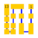
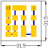
MTR Series of multi tap thin film chip resistors are designed to be used for circuit trimming through selective wire bonding in chip and wire hybrid circuits for biasing discrete transistors, as feedback resistors in microwave amplifiers and as precision voltage dividers. Because they are extremely compact and very easy to program, multi tap resistors are used both in design and prototyping as well as in production. Multi tap resistors help reduce the inventories by stocking fewer items. MTR Series of multi tap thin film resistors are manufactured on silicon substrate, 100% tested, visual inspected and packaged in waffle packs. US MICROWAVES manufacturer of high reliability microwave integrated circuits MIC technology. US Microwave offers a multitude of applied thin film products and microwave semiconductor devices: manufactures and supplies high quality standard microwave thin film circuits and microwave devices using advanced technical ceramics and semiconductor materials; Products include RF micro devices for hybrid chip and wire applications; microwave thin film circuits, custom manufacturing from customer's data, spiral chip inductors - ceramic, sapphire and quartz substrate, thin film resistors - ceramic, silicon and quartz substrates, multi-tap thin film resistors - ceramic and silicon substrates, capacitors MIS for chip and wire applications, MNOS capacitors, MOS capacitors, ceramic capacitors, Schottky diodes, PIN diodes, tunnel diodes, SRD diodes, varactor diodes and zero bias diodes, RF NPN and PNP transistors, high speed LDMOS and T MOSFET s, MMIC - RF IC s silicon and SiGe. SEMICONIX Designs and manufactures standard and custom bipolar and MOS analog devices, semiconductors, analog integrated circuits, discrete components for high performance systems such as cellular/wireless, video amplifiers, heart pacemakers and medical imaging systems. Standard semiconductor components are designed and manufactured for space, medical, telecommunications and military applications only. Company's technology road map is including SiGe epi devices for high speed RF bipolars and high speed fiber optic and optoelectronic applications. Analog devices, ASIC analog design and manufacturing: Semiconix produces a series of semi-custom bipolar analog devices in arrays that are customized by designing a specific metal interconnection mask. The arrays contain a large number of undedicated active and passive components, i.e. transistors, diodes, resistors, capacitors, MOSFET s, LDMOS, photodiodes, phototransistors, etc. Since wafers are stocked before the metal mask, the custom IC development phase is shorter and far less expensive compared to conventional full custom ICs. Customers may provide own analog design. Optoelectronic components: photodiodes, photodiodes arrays, phototransistors, position sensing devices, optocouplers, optoisolators, photodarlington, high voltage phototransistors output, Schottky infrared detectors. Discrete semiconductors: Schottky diodes, Zenner diodes, TVS, small signal bipolar transistors, high voltage bipolar transistors, matched pair bipolar transistors, small signal JFET s and MOSFETs, MCT (MOS controlled tyristors), IGBT. Semiconix 's Divisions:HTE Labs Provides Wafer Foundry, R&D support and Specialty Wafer Fab Processing to customers from semiconductors and microelectronics industry. Wafer foundry includes the following processes: 20V, 45V, 75V, 25V super-beta and high voltage dielectric isolated bipolar process. R&D support is provided in the following fields of microelectronics: thin film active and passive components technologies, flip chip technology (TiW/Cu/Cu/SnPb), sensor technologies (inertial, pressure, temperature, gas and smoke detectors), optoelectronic technologies and components, discrete and integrated circuits technology development for special applications, LiNbO3 applications like SAW, Ti diffused, light wave guides and Mach-Zender light modulators. Specialty wafer fab processing: epitaxy, SiGe, epi, diffusion and oxidation, ion implant, LPCVD and PECVD Si3N4, SiO2, platinum silicidation, photo-lithography, plasma etching, silicon micro-machining by KOH anisotropic etch, sputter depositions of Ti/Ni/Ag lift off process, Ti/Pt/Au lift off process, sputter depositions of thin film resistors: SiCr, NiCr, TaN2, silicon wafers back grind and polish followed by trimetal backside sputter depositions, gold backside sputter depositions and alloy : gold electroplating and gold bump. SEMICONWELL designs and manufacture standard and custom Integrated Passive Networks - IPN for the personal computer, telecommunications, industrial controls, automotive, avionics. The Integrated Passive Networks are a sum of resistors, capacitors, inductors, diodes and schottky diodes and are available in through hole and surface mounted packages. SEMICONWELL is suppling integrated termination, filters and ESD protection for use in mobile phones, PDAs, personal computers, notebooks, routers, hubs, internet appliances. Standard Devices - Most standard devices include resistors, capacitors, inductors, diodes and schottky diodes networks and are inventoried by the designated part numbers and can be ordered on line, from factory or from distributors. Custom Devices - Custom IPN (Integrated Passive Networks) are manufactured from customer's prints upon request. US MICROWAVES develops, manufactures and supplies high quality standard microwave thin film circuits and microwave devices including RF bipolars for hybrid chip and wire applications as follows: microwave thin film circuits, custom manufacturing from customer's data, spiral chip inductors - ceramic, sapphire and quartz substrate, thin film resistors - ceramic, silicon and quartz substrates, multi-tap thin film resistors - ceramic and silicon substrates, capacitors MIS for chip and wire applications, MNOS capacitors, MOS capacitors, ceramic capacitors, Schottky,PIN, tunnel, SRD, varactor and zero bias diodes, RF NPN and PNP transistors, high speed LDMOS and T MOSFET s, MMIC - RF IC s silicon and SiGe. |