Microwave Thin Film Circuits Layout Design Rules
US Microwaves stocks a large variety of substrates. However it offers only 2 most common standard materials for fastest turn around applications:
Alumina (Al2O3) 99.6% thin film grade ceramic substrates, available in as fired surface finishes < 4 micro inches. Standard ceramic thickness: 005", .010", .015", .020", and .025".
Quartz (SiO2) 99.9% fused silica, front side polished <1 micro inches, backside as lapped. Standard Quartz substrate thickness is 20 mils +/-1 mil.
Other materials are available: AlN aluminum nitride, BeO beryllium oxide, glass, sapphire. All ceramic substrates are also available polished with <1 micro inch surface finish on special request only.STANDARD THIN FILM METALLIZATION for microwave applications:
For fastest turn around, US Microwaves offers the following proven (over 12 years) standard high reliability MIC technology metallization:
Front Side metallization:
TaN: 50 or 100Ω/square.
TiW: 500Å ±20%.
Au: 150µ inches standard.
Back Side metallization:
TiW: 500 Å ±20%.
Au: 150µ inches standard.
This metallization scheme has proven extremely high thermal stability and corrosion resistance.
For instance, after 30 min at 450°C in air, there is no sign of metal blistering or degradation of adhesion. This test can not be passed by any metallization that includes Ni or Cu.
US Microwaves MIC circuits, can pass a dip for 15 min, 40°C, 100% H2SO4 sulfuric acid solution with ought sign of performance degradation or signs of corrosion. Again, the same test can not be passed by any metallization that includes Ni or Cu.
This metallization is compatible with AuGe, AuSn, AuSi, AuIn and conductive silver epoxies.
For special applications where temperature excursions to as high as 600°C are necessary, customers are advised to use the same high reliability standard metallization system.
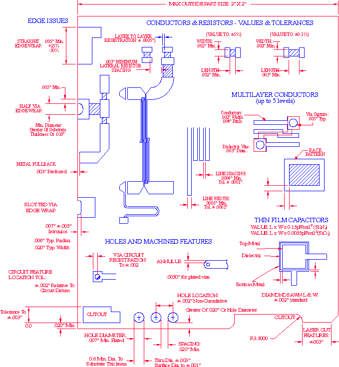
METALLIZED & PLATED LASER DRILLED VIA HOLES:
Minimum aspect ratio of 0.8:1.0 (e.g. .008" hole in a 0.010" thick substrate).
Metallized plated slots - Can be used to allow processing of wrap-around circuits.
Filled via is a process option available for application where thermal and electrical grounding is required.
Masks are produced by US Microwaves in house mask shop within 24 hours. Masks are produced by direct 1x print for devices that have minimum feature sizes of 2mil lines and spaces. Devices with less than 2 mil features are processed using the 4x stepper. Maximum circuit size in the case of 4x stepper is 0.625"x0.625" including the scribe lines. Devices with less than 1 mil features and >0.4mil are processed using the 10x stepper. Maximum circuit size in the case of 10x stepper is 0.250"x0.250" including the scribe lines. US Microwaves offers mask manufacturing services only in conjunction with the manufacturing of microwave thin film circuits. US Microwaves does NOT sell Masks. Masks are generated from AutoCAD *.dwg files.
AutoCAD *Special requirements:
Explode and purge all blocks.
Save files as DWG format (not DXF).
Make sure files are not read-only or locked.
Make sure you have the part number on both layers (conductor and resistor).
If possible, erase all unnecessary layers except conductor, resistor, outline and the dimensions information.
STANDARD MIC process DELIVERY and PRICING: On-Line Quotation
Pricing and delivery information for custom microwave thin film circuits is available on line without need of registration. The following is a quick overview of US Microwaves typical delivery for standard MIC technology and applied thin film products, however visitors are advised to check the on line quotation calculator.
Delivery is 5-10 w days ARO from customer supplied DWG file for non via thin film microwave circuits depending on the number of layers.
Delivery starts within three to four weeks ARO for circuits with laser drilled via, metallized plated via, metallized plated slots, wrap around ground connection.
Faster turn-around is available in certain cases for a premium upon special request only.
STANDARD DIMENSION SPECIFICATIONS:
Minimum line width: 0.0004"
Minimum Gap: 0.0004"
Maximum Au thickness: 200µ inches, special requests.
Minimum distance from edge of circuit to conductor: 0.001"
Minimum distance from edge of circuit to resistor: 0.002"
STANDARD TOLERANCES:
Minimum line width tolerances: ± 0.0001"
Line width tolerance on all non-critical areas: = 0.0005"
Metal thickness tolerance: ±20%
Integrated Resistor tolerance: ±10%
Circuit size tolerance: ±0.002"
For MICROWAVE THIN FILM CIRCUITS ON LINE QUOTATION please click here: On-Line Quotation